Oct 11 2012
Nanotechnology-based materials identification enables critically needed chemical metrology for nano-manufacturing
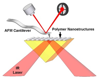
 Atomic Force Microscope Infrared Spectroscopy is a nanotechnology-based materials identification technique. (credit: University of Illinois at Urbana-Champaign)
One of the key achievements of the nanotechnology era is the development of manufacturing technologies that can fabricate nanostructures formed from multiple materials. Such nanometer-scale integration of composite materials has enabled innovations in electronic devices, solar cells, and medical diagnostics.
While there have been significant breakthroughs in nano-manufacturing, there has been much less progress on measurement technologies that can provide information about nanostructures made from multiple integrated materials. Researchers at the University of Illinois Urbana-Champaign and Anasys Instruments Inc. now report new diagnostic tools that can support cutting-edge nano-manufacturing.
"We have used atomic force microscope based infrared spectroscopy (AFM-IR) to characterize polymer nanostructures and systems of integrated polymer nanostructures," said William King, the College of Engineering Bliss Professor in the Department of Mechanical Science and Engineering at the University of Illinois Urbana-Champaign. "In this research, we have been able to chemically analyze polymer lines as small as 100 nm. We can also clearly distinguish different nanopatterned polymers using their infrared absorption spectra as obtained by the AFM-IR technique."
In AFM-IR, a rapidly pulsed infrared (IR) laser is directed on upon a thin sample which absorbs the IR light and undergoes rapid thermomechanical expansion. An AFM tip in contact with the polymer nanostructure resonates in response to the expansion, and this resonance is measured by the AFM.
"While nanotechnologists have long been interested in the manufacturing of integrated nanostructures, they have been limited by the lack of tools that can identify material composition at the nanometer scale." said Craig Prater, co-author on the study and chief technology officer of Anasys Instruments Inc. "The AFM-IR technique offers the unique capability to simultaneously map the nanoscale morphology and perform chemical analysis at the nanoscale."