Oct 8 2012
New etching method to produce 3-dimensional microstructures in silicon for the processing of light signals in telecommunications
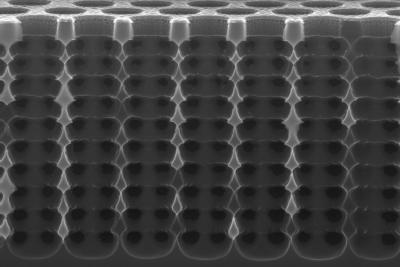
 Deep below the silicon surface, the SPRIE method produces regular structures in the micrometer range that refract light. (Photo: KIT/CFN)
In modern telecommunications, light carries digital information over kilometers within seconds. Adapted optical materials control the light signals. In the AFM journal, researchers from Berlin, Louvain, and from Karlsruhe Institute of Technology present a method to produce photonic crystals. Their optical properties are adjusted by structures of micrometer size. The method is rapid, cheap, and simple and partly uses the self-organization principle (DOI: 10.1002/adfm.201201138).
"Optical properties of materials can be influenced decisively by specific structurization," explains Andreas Frölich from Karlsruhe Institute of Technology. Silicon is used in components, e.g. filters or deflectors, for telecommunications. So far, however, all these components have been flat, i.e. two-dimensional. Entirely novel concepts might be feasible using three-dimensional components. The expenditure required to structure the silicon is very high. The structure has to be very regular in all three spatial directions and details are to have the size of about one micrometer, which corresponds to one hundredth of the thickness of a hair.
"Our new SPRIE fabrication methods uses established technologies, such as etching and innovative methods like self-organization and combines them in a very creative manner," says Martin Wegener, Professor of the Institute of Applied Physics and Institute of Nano-technology of KIT and coordinator of the DFG Center for Functional Nanostructures (CFN). The SPRIE method is applied to structure silicon on large areas in a simple and three-dimensional manner. First, a solution with micrometer-sized spheres of polystyrene is applied to the silicon surface. After drying, these spheres automati-cally form in a dense monolayer on the silicon. Upon metal coating and the removal of the spheres, a honeycomb etching mask remains on the silicon surface.
"This etching mask is our two-dimensional template for the construc-tion of the three-dimensional structure," says Frölich. The free areas are removed by etching with a reactive plasma gas. An electric field is applied to make the gas particles etch into the depth only or homogeneously in all directions." In addition, we can specifically pas-sivate the walls of the hole, which means that it is protected from further etching by a polymer layer."
Repeated etching and passivation makes the holes of the etching mask grow into the depth. With up to 10 micrometers, their depth exceeds their width by a factor of more than 10. The process steps and the electric field are adjusted precisely to control the structure of the walls. Instead of a simple hole with vertical smooth walls, every etching step produces a spherical depression with a curved surface. This curvature is the basis for the regular repeating structures of novel waveguides. "Optical telecommunication takes place at a wavelength of 1.5 µm. With our etching method, we produce a cor-rugated structure in the micrometer range along the wall." The field at closely adjacent and very deep, structured holes acts like a regular crystal that refracts in the desired manner.
The SPRIE (Sequential Passivation and Reactive Ion Etching) method can produce a three-dimensional photonic crystal within a few minutes, as it is based on conventional industrial processes. In principle, a three-dimensional structure can be generated in silicon using a freely choosable mask. This opens up new possibilities for meeting the requirements made on optical components in telecommunications. Different designs of photonic crystals are available. Some are applied as waveguides with very small curvature radii and small losses or as extremely small-band optical filters and multiplexers. In few decades, computers working with light instead of electricity might be feasible. Apart from KIT, the Belgian Université catholique de Louvain and Humboldt University, Berlin, were involved in the development.