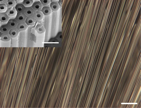
An international team of scientists in the United Kingdom and the United States have developed a new chemical process, where a non-crystalline form of silicon is embedded into the long, ultra-thin pores of optical fibers. This is the first technique to apply high-pressure chemistry for the manufacture of advanced films and wires of this specific silicon semiconductor assisting scientists in the production of more flexible and efficient optical fibers.
 A new chemical technique developed at Penn State, the first of its kind, can help scientists to make more-efficient and more-flexible optical fibers.
The assessments prepared by an international team directed by John Badding, a professor of chemistry at Penn State will be published in a upcoming print version of the Journal of the American Chemical Society.
Pier J. A. Sazio, a team leader from the University of Southampton, UK says that although the low-pressure plasma reactor technique can be employed for producing solar cells by depositing hydrogenated amorphous silicon onto a surface, the silane precursor molecules cannot to be thrust into the long, thin holes of the optical fibers. Hence, a high-pressure technique is required for forcing the molecules of silane through the fiber, thereby converting them into amorphous hydrogenated silicon. This technique is distinctive as it allows the silane to decompose into hydrogenated amorphous silicon.
Noncrystalline silicon-based optical fiber has varied applications. Some of the advantages include utilization in telecommunications devices, conversion of laser light into different infrared wavelengths. Infrared lights are employed for improving chemical-sensing tools in detecting pollutants and environmental toxins, military countermeasure devices, and surgical techniques. This research will also be used for the development of the existing solar-cell technology.