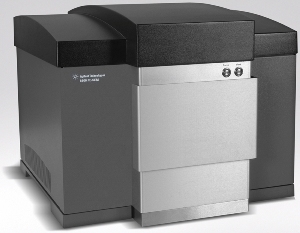
Agilent Technologies has launched a new, compact Agilent 8500 FE-SEM (Field Emission Scanning Electron Microscope) for research applications.
The scanning electron microscope allows researchers to perform low-voltage imaging in their laboratory. The 8500 FE-SEM is optimized for high resolution and high-surface contrast that are normally found in expensive and large-sized field emission microscopes.
 Agilent FE-SEM 8500
The Agilent 8500 FE-SEM has a similar size like the laser printer and provides a number of imaging techniques to improve the surface contrast. The 8500 FE-SEM enables nanoscale features to be viewed on biomaterials, thin films and polymers.
With the 8500 FE-SEM, users do not have to coat the samples or resort to pressure operation. The former can cover the nanoscale features, while the latter can reduce the resolution. The 8500 FE-SEM utilizes a microchannel plate detector, which offers topographic imaging to improve the surface detail. The 8500 FE-SEM has an electrostatic lens design that provides continuous performance without requiring constant retuning.
Agilent employs microfabrication techniques to design an electrostatic electron beam column that is integrated with a field emission electron source for the 8500 FE-SEM.
Agilent Technologies’ Operations Manager, Jeff Jones, stated that the 8500 FE-SEM provides researchers a variety of advanced capabilities that were previously found only in centralized FE-SEMs.