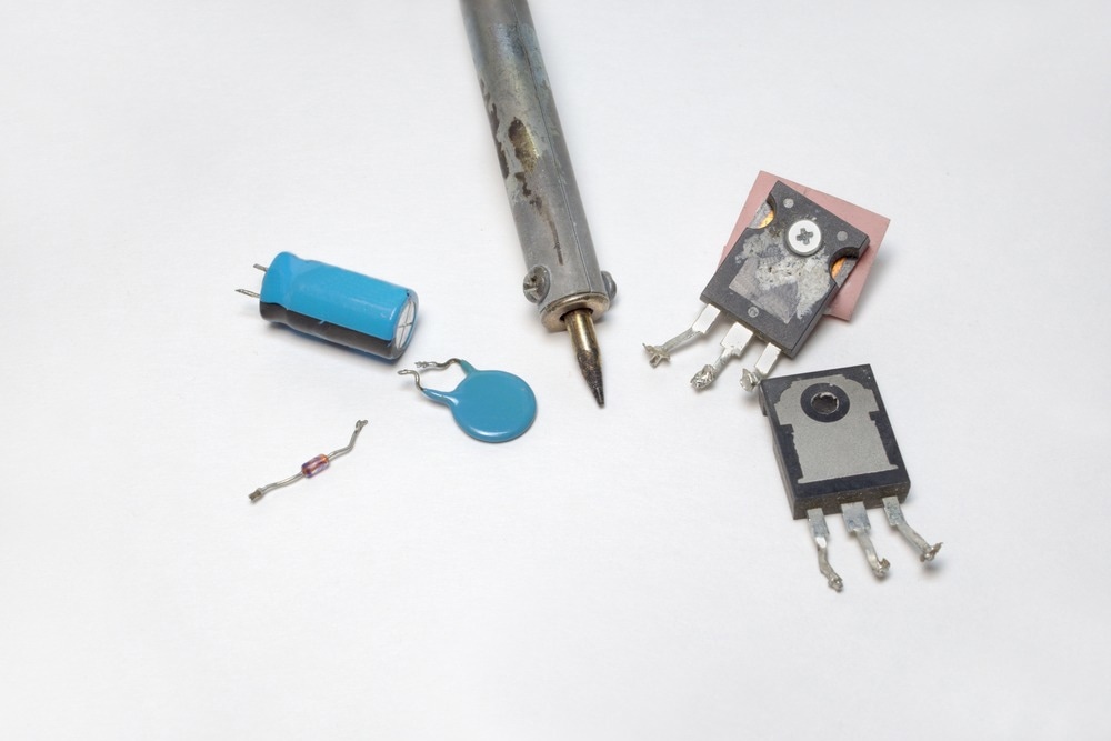
Similar to other junction diodes, the Schottky Barrier Diode is a type of semiconductor diode that is employed in many electronic applications requiring low voltage and high current operations.

Image Credit: theLIMEs/Shutterstock.com
The Schottky Diode is named after the German physicist Walter H. Schottky, who first observed an irregularity in the thermionic emission in a vacuum tube. Thermions are electrons or ions released by a material under extreme heat. The discovery of the irregularity, referred to as the Schottky effect, led to the development of Schottky Barrier diodes.
Semiconductor Diodes
A PN-junction diode is produced by connecting a p-type and an n-type semiconductor together, enabling it to be operated as a rectifying tool. When forward-biased, the depletion region in a semiconductor is significantly reduced, enabling current flow in the forward direction. When reverse-biased, the increase in the depletion region blocks the current flow.
The resistance of the junction barrier is changed depending on whether the pn-junction is biased forward or backward using an external voltage. As a result, the resistance value of the junction affects the voltage-current relationship of a conventional pn-junction diode. As a nonlinear device, the pn-junction diode's DC resistance will change depending on the biasing voltage and the current flowing through it.
Conventional diodes are manufactured with semiconductors such as silicon or germanium.
For silicon diodes, the voltage needed for forward conduction to happen is roughly 0.65 to 0.7 volts. When a junction is forward biased, conduction through the junction does not begin until the external biasing voltage hits the "knee voltage," at which time current increases fast.
Depending on how the silicon junction diode was doped during manufacturing and whether it is a small diode or a much bigger rectifying diode, the knee voltage for practical silicon junction diodes can range from 0.6 to 0.9 volts. However, a normal germanium diode has a knee voltage that is significantly lower, around 0.3 volts, making it more suitable for small signal applications.
Schottky Barrier Diodes
Schottky Barrier Diodes are built utilizing a metal electrode bonded to an N-type semiconductor that has undergone light doping, as opposed to a standard pn-junction diode, which is composed of a P-type and N-type semiconductor joined together.
The Schottky barrier diode has no depletion layer since it is built with doped silicon on one side and a metal compound on the other of its junction, in contrast to normal pn-junction diodes, which are bipolar devices.
The type of metal compound and semiconductor material used in this metal-semiconductor junction's construction will have a significant impact on its width and, consequently, its electrical characteristics. However, when forward-biased, electrons move from the n-type material to the metal electrode, allowing current to flow. Therefore, the majority of carriers' drift produces the current that passes through the Schottky diode.
A highly conductive silicon and metal compound known as "Silicide" is the most popular contact metal utilized in the manufacture of Schottky diodes. The ohmic resistance of this silicide metal-silicon contact is relatively low, allowing more current to flow and resulting in a forward voltage drop of only about 0.4V while conducting. The forward voltage decreases caused by various metal compounds range in magnitude from 0.3 to 0.5 volts.
Schottky Barrier Photodetectors
The Schottky photodiode uses the same fundamental design and fabrication methods as the conventional Schottky barrier diode.
Due to its dual photo-detection modes of operation, the Schottky photodiode is a special type of photodetector with the following characteristics:
- From energy gap excitation between bands, the semiconductor produces electron pairs.
- Through the Schottky barrier, carriers are emitted from the metal into the semiconductor. A common name for this is internal photoemission.
The intrinsic layer of the PIN photodiode performs a similar function to that of the metal-semiconductor junction. As a result, it offers a greater surface for the capture of photon energy.
Applications Using the Schottky Barrier Photodetectors
Just like the Schottky barrier diode, the Schottky photodetector works best with silicide and advanced silicon technology. As a result, these photodiodes are frequently used as the image-sensing photodetector in CCDs, or charge-coupled devices.
Both the Schottky photodiode and the CCD transfer gate, which work with silicon technology, can be combined into a single device. To enable the data from many Schottky photodetectors to be shifted out of the overall chip in a controlled manner, the CCD itself acts as a shift register. This provides a way to extract large amounts of data from the array of photodiodes with a reasonable number of leads on the integrated circuit.
Schottky diodes and Schottky photodiode detectors are fast replacing other rectification components as the go-to choice in low voltage, high current solar panels, and renewable energy applications.
However, Schottky photodiodes do have some drawbacks. As a result of light reflection and absorption in the metal layer, they are typically less effective than PIN photodiodes at longer wavelengths. Antireflection coatings are frequently used to reduce light reflection. Further development is being continuously pursued to improve the performance of Schottky barrier photodetectors.
More from AZoOptics: What is Quantum Microscopy?
References and Further Reading
Richard S. Quimby. Photonics and Lasers: An Introduction 17 March 2006 ISBN:9780471719748 |DOI:10.1002/0471791598
Electronics Tutorials. The Schottky Diode. [Online]. ElectronicsTutorials. Available at: https://www.electronics-tutorials.ws/diode/schottky-diode.html
Electronics Notes. Schottky Photodiode. [Online]. ElectronicNotes Available at: https://www.electronics-notes.com/articles/electronic_components/diode/photodiode-detector-schottky.php
Disclaimer: The views expressed here are those of the author expressed in their private capacity and do not necessarily represent the views of AZoM.com Limited T/A AZoNetwork the owner and operator of this website. This disclaimer forms part of the Terms and conditions of use of this website.