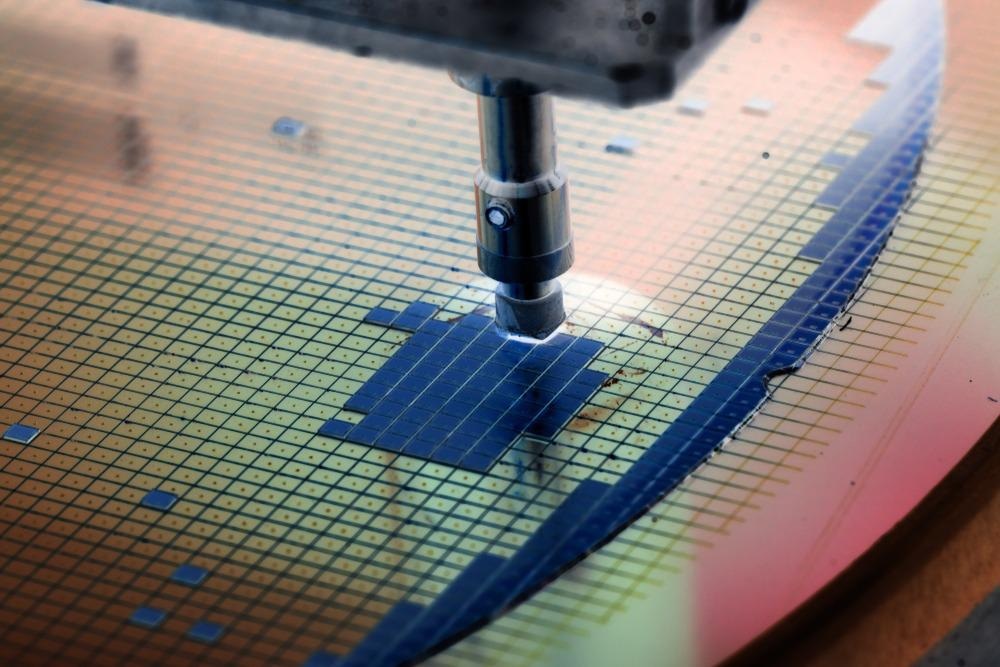
Optical properties of semiconductors are harnessed to develop some of the most widely used technology in the world. Some prominent optical semiconductors are transistors, light-emitting diodes (LED), laser diodes and infrared LEDs. Semiconductor transistors support the foundation of integrated circuits (ICs) used in most electronic devices.

Image Credit: Macro photo/Shutterstock.com
LEDs are used in display screens, lighting, traffic lights and electronic devices. Laser diodes are used for writing DVDs, optical fiber communication and 3D sensors. TV remote controls, security cameras and vehicle cameras use IR LEDs.
Diode lasers are a cornerstone in the development of quantum technology. A diode laser is a semiconductor laser based on laser diodes and is heavily employed for laser cooling atoms and addressing specific atomic transitions.
Types of Semiconductors
Semiconductors are classified as materials that exhibit electrical conduction ability that lies between conductors and insulators. Some examples of semiconductor elements are silicon (Si), indium (In), germanium (Ge) and arsenic (As).
Semiconductors are categorized into intrinsic (chemically pure) semiconductors and extrinsic semiconductors.
In intrinsic semiconductors, the number of electrons and holes is determined by the properties of the material itself instead of the impurities. Electrons are the fundamental negatively charged carriers and the holes are the positively charged vacancies in the semiconductor. In intrinsic semiconductors, the number of excited electrons is equal to the number of holes.
In an extrinsic semiconductor, its electrical and optical properties are modified by introducing specific impurities.
Impurities change the concentration of electrons or protons to accomplish specific requirements. Also, known as compound semiconductors, these doped semiconductors are suitable for electrical and optoelectronics applications. Examples of extrinsic semiconductors include gallium arsenide (GaAs), indium phosphide (InP) and gallium nitride (GaN).
Optical Properties of Semiconductors
The optical properties of semiconductors can be divided into optical lattice properties and electronic properties. Optical lattice properties involve the vibrations of lattice-ionic crystals. They exhibit strong absorption and reflection in the infra-red part of the electromagnetic spectrum as a result of the interaction of light with optical phonons. Phonons refer to lattice vibrations.
Optical electronic properties concern processes involving the electronic states of solids. Electronic states are the energy bands in a semiconductor. The valence band and the conduction band are the key energy states within a semiconductor that is exploited for developing technological devices.
Valence Band and Conduction Band of a Semiconductor
The valence band is the outermost energy level of the semiconductor that is occupied by electrons. The electrons in the orbitals of the valence band can be excited into the conduction band by applying an appropriate amount of energy.
The conduction band comprises electron orbitals, where the valence band electrons can jump to when excited. Electrons in the conduction band orbitals have enough energy to move freely within the semiconductor. When an electron is excited from the valence band to the conduction band, a hole is created in its vacancy. Positively charged holes have the ability to move freely within the material as well.
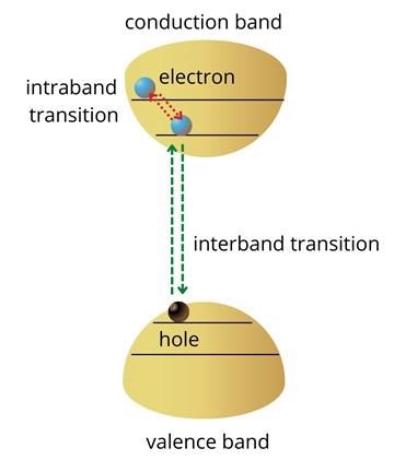
Electrons in semiconductors make transitions between two energy states when excited with photons. This process is similar to optical transitions in atoms. Transitions between the conduction band and the valence band are termed interband transitions. Absorption, spontaneous emission, and stimulated emission can all take place between the conduction band and valence band.
Absorption and Emission in Semiconductors
Optical absorption in a semiconductor occurs when a photon is absorbed. The condition for absorption is that the photon energy has to be greater than or equal to the bandgap energy. The bandgap energy is the energy difference between the valence and conduction bands. The absorption method generates an electron in the conduction band and a hole in the valence band.
Electrons created at energies higher than the band edge will rapidly ease to the lowest conduction band energy states.
Similarly, holes created deep in the valence band will move to the top states of the valence band as shown in figure 1. The transition of electrons between energy levels within the conduction or valence band is referred to as intraband transitions. Intraband transitions are also exploited to develop optoelectronic technology.

Figure 1: Energy band structure of a semiconductor. Image Credit: Ilamaran Sivarajah
Spontaneous emission and stimulated emissions also occur in semiconductors. Spontaneous emission, also referred to as optical recombination, happens when an electron in the conduction band relaxes back into the valence band and emits a photon in the process.
Spontaneous emission happens naturally and randomly without any interactions with additional photons. In stimulated emission, additional optical pumping facilitates the electron decay from the conduction band to the valence band.
Outlook
The optical properties of semiconductors are manipulated to develop light-emitting and light-receiving devices. For example, diode lasers are light-emitting devices that are used for many applications.
Laser cooling and addressing atoms, molecules and semiconductors are a foundational platform in quantum computing and sensing.
Advanced research is conducted on light-receiving devices such as solar cells and single-photon detectors. Efficient solar cells will have an immense impact on the move toward clean and renewable energy production. Single-photon detectors are a critical development in the next wave of quantum devices.
Quantum dots are another semiconductor-based nanoparticle with applications in many industries. They are emerging as promising probes for ultrasensitive detection of cancer biomarkers.
References and Further Reading
Lu, W., Fu, Y. (2018). Introduction to Physics and Optical Properties of Semiconductors. In: Spectroscopy of Semiconductors. Springer Series in Optical Sciences, vol 215. Springer, Cham. https://doi.org/10.1007/978-3-319-94953-6_2
Mônica A. Cotta, ACS Applied Nano Materials 2020 3 (6), 4920-4924 DOI: 10.1021/acsanm.0c01386
Sagadevan Suresh, Semiconductor Nanomaterials, Methods and Applications: A Review, Nanoscience and Nanotechnology, Vol. 3 No. 3, 2013, pp. 62-74. doi: 10.5923/j.nn.20130303.06.
Wagner MK, Li F, Li J, Li XF, Le XC. Use of quantum dots in the development of assays for cancer biomarkers. Anal Bioanal Chem. 2010 Aug;397(8):3213-24. doi: 10.1007/s00216-010-3847-9. Epub 2010 Jun 9. PMID: 20532875.
Disclaimer: The views expressed here are those of the author expressed in their private capacity and do not necessarily represent the views of AZoM.com Limited T/A AZoNetwork the owner and operator of this website. This disclaimer forms part of the Terms and conditions of use of this website.