Image Credit: Elizaveta Galitckaia/Shutterstock.com
Scanning optical microscopy is a microscopy technique that sits within the broader category of scanning probe microscopy. It was developed in the 1980s to enable the study of properties such as refractive index, chemical structure, and local mechanical and chemical stresses at the scale of nanometers.
Introduction to Scanning Optical Microscopy
Scanning optical microscopy is a method for the investigation of nanostructures in samples. It enables researchers to break the far-field resolution limit, and so is also referred to as near-field scanning optical microscopy or, sometimes, as scanning near-field optical microscopy.
It works by exploiting evanescent waves’ unique properties. These are oscillating electromagnetic fields with energy that is spatially concentrated close to the source, however, they are not electromagnetic waves.
In the scanning optical microscopy technique, light from an excitation laser is focused with confocal lenses through an aperture whose diameter is smaller than the wavelength of the excitation. This creates an evanescent field (near-field) on the other side of the aperture.
The sample can then be scanned at a minutely small distance below the aperture. When this is done, the transmitted or reflected light’s optical resolution is only limited by the aperture’s diameter. This results in lateral resolutions of as little as 20 nanometers, and vertical resolutions of between 2 and 5 nanometers.
As well as refractive index, chemical structure, and local stress, this contrast mechanism can also be adapted for the study of dynamic properties at a sub-wavelength scale.
Theory: Overcoming the Rayleigh Criterion Limit
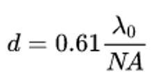
Due to diffraction, the optical component’s resolving capability is limited by each image point’s spreading out; the final image does not correspond exactly to the object under study – unless the optical component’s aperture is large enough to collect all light that has been diffracted. Therefore, minimum resolution in conventional optical microscopy is limited by aperture size. This limit is expressed by the Rayleigh criterion:

Λ0 here represents the wavelength inside the vacuum, while NA is the optical component’s numerical aperture. For conventional optical microscopy, Λ0/2 is the usual resolution limit.
However, this only considers light that has been diffracted into the far-field and which therefore propagates the absence of restrictions. Scanning optical microscopy manipulates non-propagating, evanescent fields that occur at extremely close distances to the object’s surface to overcome the observation limitations expressed by the Rayleigh criterion.
These evanescent fields are carriers of high-frequency spatial data which researchers can study to understand the object’s nanostructure and properties. The intensity of such evanescent fields undergoes exponential drop-off with increased distance from the object’s surface.
This means that the scanning optical microscope sensor must be placed in the near field zone, only a few nanometers away from the surface of the object. In turn, this means that scanning optical microscopy is best suited for surface inspection.
The microscope’s sensor or detector is scanned across the sample using the raster scanning technique. This takes place through the manipulation of piezoelectric forces. Raster scanning can be performed at a consistent height (distance from the object’s surface), or it can be programmed to regulate height over the object using precise feedback mechanisms.
Components and Composition of a Scanning Optical Microscope
The instruments commonly required for scanning optical microscopy are:
- A light source
- Scanning tip
- Detector or sensor
- An optional feedback mechanism
- A piezoelectric sample stage or platform
Lasers focused into an optical fiber through a polarizer, beam splitter and coupler typically provide the light source. Stray light is removed from returning (reflected) light with the polarizer and beam splitter.
The scanning tip is commonly an optical fiber coated with metal. The optical fiber is pulled or stretched and the tip is left uncoated. Standard atomic force microscopy cantilevers can also be used if modified with a hole in the middle of the pyramidal tip.
Optical detectors that are standard in microscopy can be used. These include avalanche photodiode, photomultiplier tube (PMT), or CCD. However, some scanning optical microscopy techniques such as Raman scanning optical microscopy require more stringent detectors.
References and Further Reading
Sheppard, Colin J.R. (2020) “Scanning Optical Microscopy.” Advances in Imaging and Electron Physics. [Online] https://doi.org/10.1016/bs.aiep.2019.11.001.
Wilson, T. (1985) “Scanning Optical Microscopy.” The Journal of Scanning Microscopes. [Online] https://doi.org/10.1002/sca.4950070203.
Disclaimer: The views expressed here are those of the author expressed in their private capacity and do not necessarily represent the views of AZoM.com Limited T/A AZoNetwork the owner and operator of this website. This disclaimer forms part of the Terms and conditions of use of this website.