Jul 13 2020
An in-depth understanding of the fundamental science behind familiar techniques used to create quantum dots, which are tiny semiconducting nanocrystals, could help minimize the guesswork of existing practices used by material scientists to develop better digital displays and solar panels.
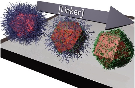
 In the solvent-dominated regime, the dots are capped with long oleic acid molecules, which hamper the flow of electricity. After the transition, these are replaced by linker molecules, allowing the dots to conduct electricity efficiently. From left to right is the solvent-dominated regime, the transition regime, and the linker-dominated regime. Image Credit: © 2020 Ahmad R. Kirmani.
Quantum dots measure only one-billionths of a meter wide and are often prepared in solution and coated or sprayed as an ink to form a thin electrically conducting film used to develop devices.
But finding the best way to do this has been a matter of trial and error.
Ahmad R. Kirmani, Material Scientist, KAUST
In collaboration with fellow KAUST researchers and those from the University of Toronto, Canada, he has shown why specific well-known techniques can drastically enhance the performance of the film.
Based on their size, quantum dots emit and absorb different wavelengths of light. This enables them to be tuned to serve as highly efficient absorbers in solar panels, or to emit various colors for a display, merely by increasing or decreasing the size of the crystals.
In general, the dots are grown from sulfur and lead in solution. Since the properties of the dots are based on their size, it is crucial to halt their growth at the right time. This is achieved by the addition of special molecules to cap their growth. In general, engineers use oleic acid molecules, each consisting of 18 carbon atoms, which attach to the surface of the crystal, similar to hairs, thereby blocking the growth.
This leads to the formation of a solution of dots appropriate for coating to develop a film. However, this film is not a good conductor of electricity as the long acid molecules hinder the flow of electrons between nanocrystals. Hence, shorter molecules are added by engineers.
Such “linkers” include only about two carbon atoms per molecule. The linkers act as a substitute for the long capping molecules, thus increasing the conductance.
The method has been used for a couple of decades, but nobody had investigated exactly what happens.
Ahmad R. Kirmani, Material Scientist, KAUST
Kirmani and his colleagues discovered that by using a microbalance to track the exchange of oleic acid for linkers at the time of transition. By scattering X-rays from the dots, they quantified the spacing between them. Moreover, they recorded the change in density, thickness, and optical absorption characteristics of the film.
Instead of a smooth transition in the properties of the film, they observed a sudden jump—marking a phase transition. When all the acid molecules were roughly displaced by the linkers, the dots suddenly come close together, and there is an abrupt increase in the conductivity.
Kirmani believes other research teams will be motivated to further investigate, probably by inhibiting the transition process almost midway and adding different molecules to the dot surface to observe what innovative features appear.
There is a lot of potential in taking this understanding to new paradigms for new technologies.
Ahmad R. Kirmani, Material Scientist, KAUST
Journal Reference:
Kirmani, A. R., et al. (2020) Optimizing Solid-State Ligand Exchange for Colloidal Quantum Dot Optoelectronics: How Much Is Enough? ACS Applied Energy Materials. doi.org/10.1021/acsaem.0c00389.