Mar 1 2019
Researchers from the University of California, Berkeley tested experimental photonic switches, revealing their potential to achieve the aim of completely optical, high-capacity switching for next-generation high-speed data transmission networks. The switch created and tested for this study exhibited potential not observed earlier in photonic switches.
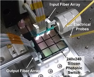
 Photo of the fabricated 240 x 240 silicon photonic switch on the characterization setup. (Image credit: Tae Joon Seok)
As part of a paper presentation at OFC: The Optical Fiber Communications Conference and Exhibition, to be held between March 3rd and 7th, 2019, in San Diego, California, United States, scientist Tae Joon Seok and his team will describe the successful scale-up of a 240 x 240 integrated silicon photonic switch. The name of the device arises from the fact that it accepts 240 optical communication input channels and sends them into 240 output channels.
The researchers used experimental photonic switches developed at the Marvell Nanofabrication Laboratory at UC Berkeley and showed a signal loss lower than any reported earlier, stated Seok, an assistant professor at the Gwangju Institute of Science and Technology in South Korea and a visiting scholar at UC Berkeley.
Addressing Industry Needs with Advanced Optical Switching
Long ago, the telecommunications industry switched over to fiber-optic technology as an optimized solution to satisfy burgeoning demands for data transmission of greater capacity and higher speeds over the old electrical copper wires. Currently, a similar uprising is happening at the points at which messages transmitted over long-haul fibers are sent and received. In the place of power-craving electrical switches that need optical-electrical-optical conversions and lead to signal loss, scientists are creating and deploying photonic switches to enhance the transmission quality and connect a single transmission to tens or even thousands of servers.
Specifically, silicon-based photonic switches powered by sophisticated complementary metal-oxide semiconductor (CMOS) technology are gaining increased attention from scientists as a robust platform because of their high capacity and low cost. Their abilities to be alternatives to electrical switches will soon encounter scalability limits in energy efficiency and performance. Researchers are now striving to achieve this potential by overcoming limitations in relation to the size of existing silicon photonic chips and enhance their performance.
Recently, many research groups competitively reported silicon photonic switches with large input/output port counts.
Tae Joon Seok, Assistant Professor, Gwangju Institute of Science and Technology; Visiting Scholar, UC Berkeley.
However, due to the limitations of the lithography tools essential for etching the desired geometric patterns on the silicon wafers that are used as a base for the integrated chips, a silicon photonic chip’s physical size has been restricted to 2–3 cm.
Seok and his team solved this problem by employing a process called lithography stitching, which involves making a wafer-scale 240 x 240 silicon photonic switch by linking nine 80 x 80 switch blocks together in a 3x3 array, using three input and three output coupler blocks. The switches created by the experiment coupled incoming and outgoing light into and from the chip via grating couplers. Electrical probes were used for actuating the switch cells.
The size of the ensuing switch area was 4 cm x 4 cm—almost doubling the size of current silicon photonic switches. “To the best of our knowledge, this is the largest integrated photonic switch ever reported on any platform,” stated Seok.
Results measured from the experimental switch were also found to be record-breaking.
The on-chip loss to port-count ratio (0.04 dB/port) is the lowest demonstrated. This technology can be applied not only to silicon photonic switches but also to any silicon photonics applications that require ultra-large-scale devices such as programmable photonic processors, and so on.
Tae Joon Seok, Assistant Professor, Gwangju Institute of Science and Technology; Visiting Scholar, UC Berkeley.