Jan 18 2019
Researchers at the University of Twente have been successful, for the first time, in linking two parts of an electronics chip with the help of an on-chip optical link. A light connection can, for instance, be a safe means to link high-power electronics to digital control circuitry on one chip, with no direct electrical connection.
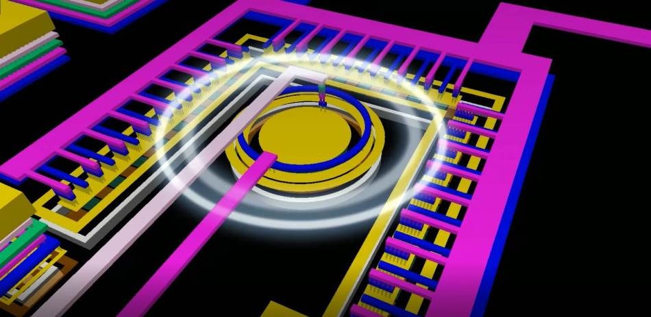
 Artist impression of the optocoupler, the round structure is the detector (Single Photon Avalanche Diode), the light source (Avalanche Mode LED) has the shape of a horseshoe. (Image credit: University of Twente)
So far, an optical link using standard silicon chip technology was not possible. Vishal Agarwal, a UT PhD student, managed to make it possible. He successfully developed a very small optocoupler circuit that offers a data rate of Megabits per second in an energy-efficient manner.
One part of a chip can be isolated from another using light: although the two different worlds can communicate, they are not connected electrically. In “smart power” chips, it is feasible to isolate the high-power part from the digital control circuits. This isolation ensures safe operation in applications such as automotive and medical electronics. This isolation is done using a device known as “optocoupler”; however, to date, this device is bulky and is separated from the actual chip. The desire to have an on-chip optocoupler has now been accomplished by Vishal Agarwal. It is possible to incorporate his optocoupler with the electronics using standard chip technology (CMOS). Its size is approximately 0.008 mm2 in size and utilizes minimal energy.
Avalanche
It is not at all trivial to integrate a light source and a light detector on a chip. Generally, unique materials will be required that cannot just possibly be introduced into the CMOS process. Silicium by itself is not a good light source. A silicon LED on a chip would release some infrared light with low efficiency, whereas a silicon detector does not work well with infrared light. For a good connection, this is not at all a good place to start. Earlier research by UT PhD student Satadal Dutta, however, showed that it is possible to achieve better results by connecting the silicon LED “the wrong way.” Consequently, an avalanche effect would take place, which leads to the emission of visible light. Similarly, a light detector can be created at which a single photon can stimulate an avalanche. The outcome is an efficient optical connection.
Efficient Design
Although the principle worked, the challenge now for Agarwal was to develop an electronic circuit that controls both the LED and the detector in an optimal way, optimizing for speed, energy consumption, and space consumption on the chip. For instance, how much voltage is required to operate the “Avalanche Mode LED” (AMLED) and the “Single Photon Avalanche Diode” (SPAD) in the most efficient manner, which brings about a good connection without wasting light? How to place the light source and light detector on the chip to obtain the maximum efficiency? In his theory, Agarwal presents an optocoupler that can be fully incorporated in CMOS, with a data rate of about 1 Megabit per second and least energy consumption. According to Agarwal, the data rate can be increased by at least tenfold for several applications despite the fact that they already have an acceptable data rate.
The study has been carried out by two Electrical Engineering groups: Integrated Circuit Design (Digital Society Institute), headed by Bram Nauta and Integrated Devices and Systems (MESA+ Institute) headed by Prof Jurriaan Schmitz. Thus, the fundamental physics of the connection and the actual design could be integrated in the best possible way.