Apr 23 2018
Physicists at the University of Warwick have managed to literally squeeze out more power from solar cells by physically deforming each of the crystals in the semiconductors used by photovoltaic cells. Details of their research have been published in the April 19, 2018, issue of the journal Science (via the Journal's First Release pages).
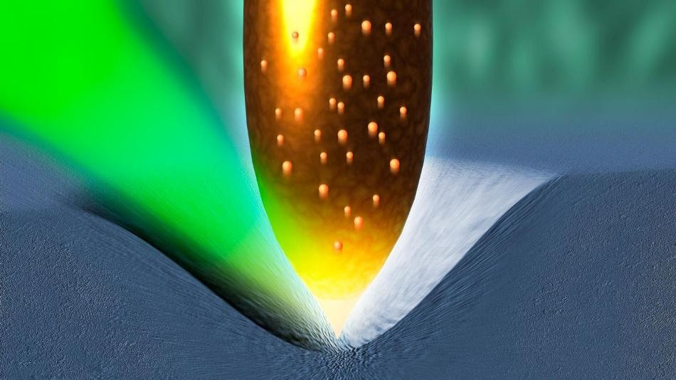
 This is an artist’s impression of squeezing more power out of solar cells by physically deforming each of the crystals in the semiconductors used by photovoltaic cells. (Image credit: University of Warwick/Mark Garlick)
The paper titled "Flexo-Photovoltaic Effect" was written by Professor Marin Alexe, Ming-Min Yang, and Dong Jik Kim, all of whom are a part of the Department of Physics at the University of Warwick.
The researchers studied the physical limitations on the existing design of most commercial solar cells which place an absolute limit on their productivity. A majority of commercial solar cells are formed of two layers forming at their boundary a junction between two kinds of semiconductors, n-type with negative charge carriers (electrons) and p-type with positive charge carriers (holes which can be filled by electrons).
The junction of the two semiconductors sustains an internal field splitting the photo-excited carriers in opposite directions when the light is absorbed, generating a current and voltage across the junction. Without such junctions, the energy cannot be harvested and the photo-excited carriers will just rapidly recombine removing any electrical charge.
That junction between the two semiconductors is central to obtaining power out of such a solar cell but it has an efficiency limit. This Shockley-Queisser Limit means that of all the power contained in sunlight falling on an ultimate solar cell in perfect conditions only a maximum of 33.7% can ever be converted into electricity.
There is, however, another method where certain materials can collect charges generated by the photons of the sun or from elsewhere. The bulk photovoltaic effect takes place in some insulators and semiconductors where their lack of flawless symmetry around their main point (their non-centrosymmetric structure) allows generation of voltage that can be, in fact, larger than the band gap of that material (the band gap can be defined as the gap between the valence band highest range of electron energies in which electrons usually exist at absolute zero temperature and the conduction band where electricity can flow).
Unfortunately, the materials that are identified to display the anomalous photovoltaic effect have very low power generation efficiencies, and are never employed in practical power-generation systems.
The Warwick team speculated if it was possible to use semiconductors that are effective in commercial solar cells and control or push them in some way so that they too could be forced into a non-centrosymmetric structure and probably thus also benefit from the bulk photovoltaic effect.
In this research, they decided to attempt pushing such semiconductors into shape using conductive tips from atomic force microscopy devices to a "nano-indenter" which they then used to squeeze and deform separate crystals of strontium titanate (SrTiO3), silicon (Si), and titanium dioxide (TiO2).
They discovered that all three could be deformed in this manner to also provide them a non-centrosymmetric structure and that they were indeed then able to deliver the bulk photovoltaic effect.
Extending the range of materials that can benefit from the bulk photovoltaic effect has several advantages: it is not necessary to form any kind of junction; any semiconductor with better light absorption can be selected for solar cells, and finally, the ultimate thermodynamic limit of the power conversion efficiency, so-called Shockley-Queisser Limit, can be overcome. There are engineering challenges but it should be possible to create solar cells where a field of simple glass based tips (a hundred million per cm2) could be held in tension to sufficiently de-form each semiconductor crystal. If such future engineering could add even a single percentage point of efficiency it would be of immense commercial value to solar cell manufacturers and power suppliers.
Professor Marin Alexe, The University of Warwick