Sponsored by PolytecReviewed by Maria OsipovaJan 30 2023
Accurate die placement and attachment are critical for process stability and the resultant component quality in epoxy die bonding and other similar die attach processes. The adhesive thickness, also known as bond line thickness (BLT), is critical for a reliable die attach to a lead frame or other substrate.
Polytec TopMap surface profilers allow for the automatic and reliable determination of die orientation on the lead frame, including die tilt and bond line thickness measurement. This non-contact measuring approach allows for quick, easy, and dependable quality control of the die bonding process.
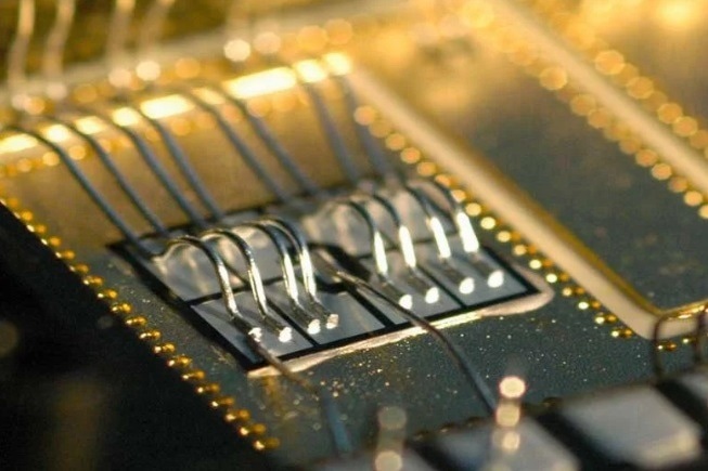
Image Credit: Polytec
Characterizing QFN Packages (Quad-Flat No-Leads)
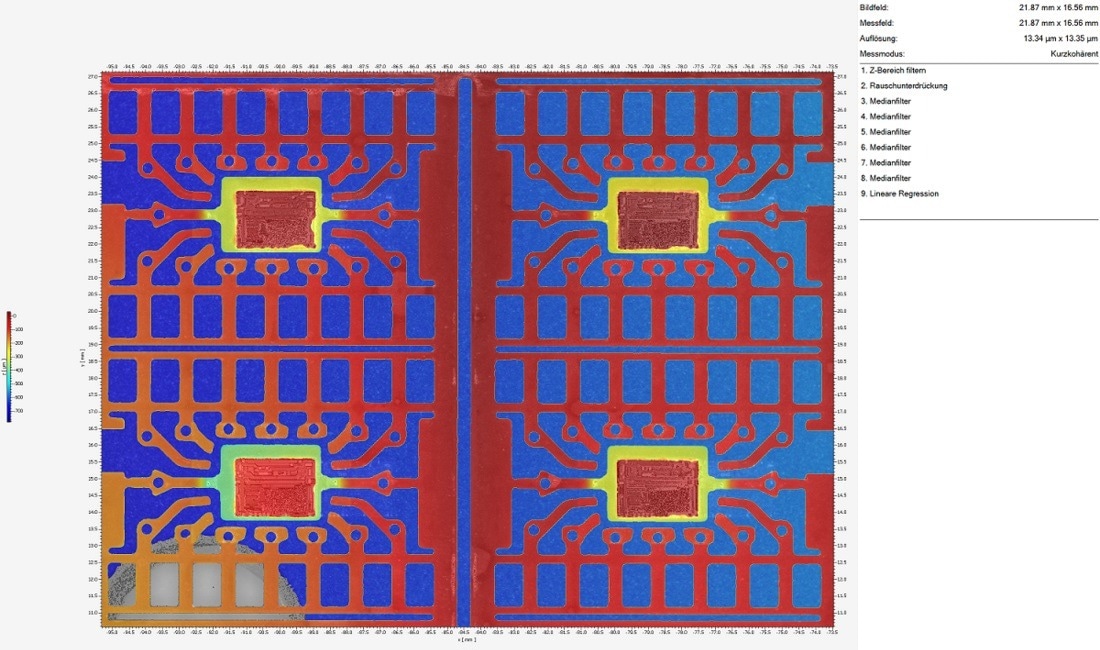
Polytec’s 3D surface metrology technologies are simple to incorporate into manufacturing lines and also provide systematic and high-resolution in-process measurement in expoy die bonding processes. Typical measurements include bond line thickness measurement (BLT), die tilt determination, torsional information, BLT height or die/chip placement, and relative measurement to a reference position.
The die attach fillet is an excess climbing on the edge of the die in quad-flat no-leads (QFN) packages, which is one of the most common chip connect types in integrated circuits. It gives the die edges mechanical strength.
The beneficial and optimized parameters, like the fillet’s height from the pad, width, slope of rise, and slope angle, can be determined using the measured bond line thickness.
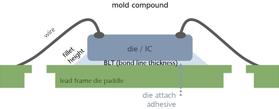
Scheme of epoxy die bonding on IC, showing die attach on the lead frame. Image Credit: Polytec
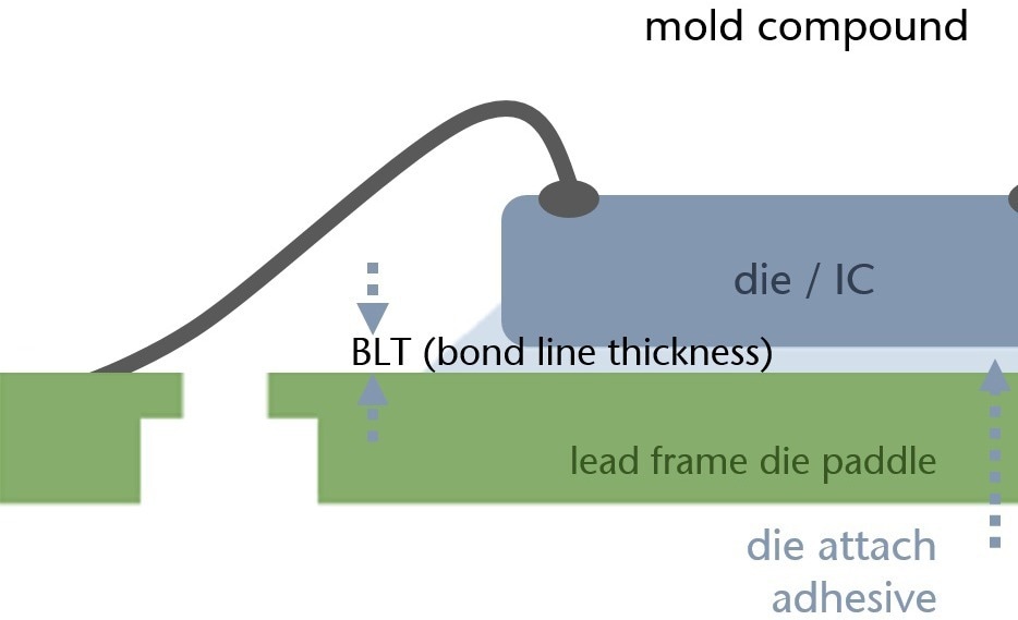
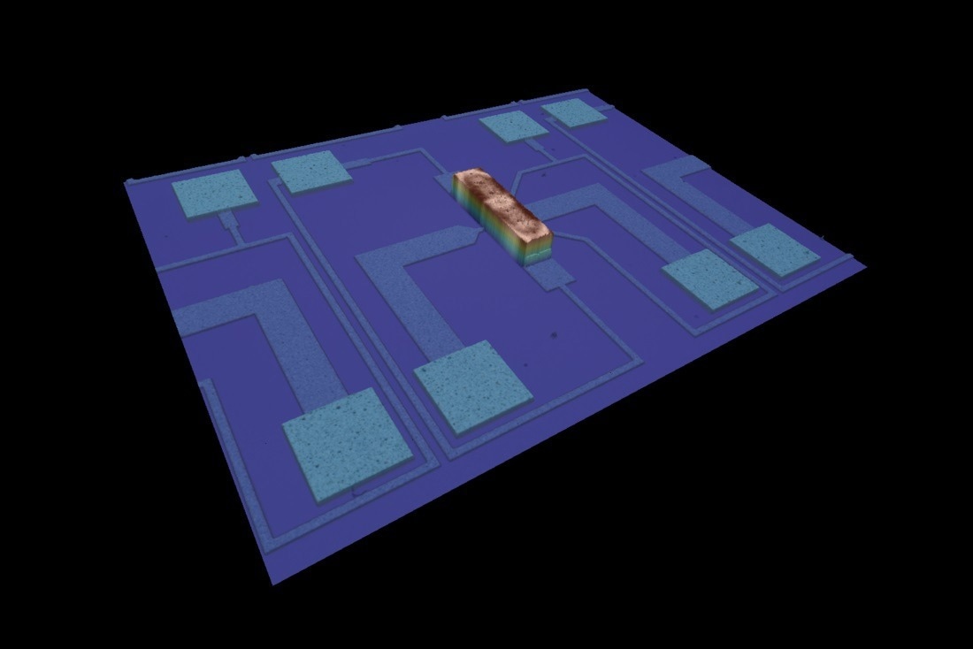
Determining bond line thickness as key quality indicator for the die bonding process. Image Credit: Polytec
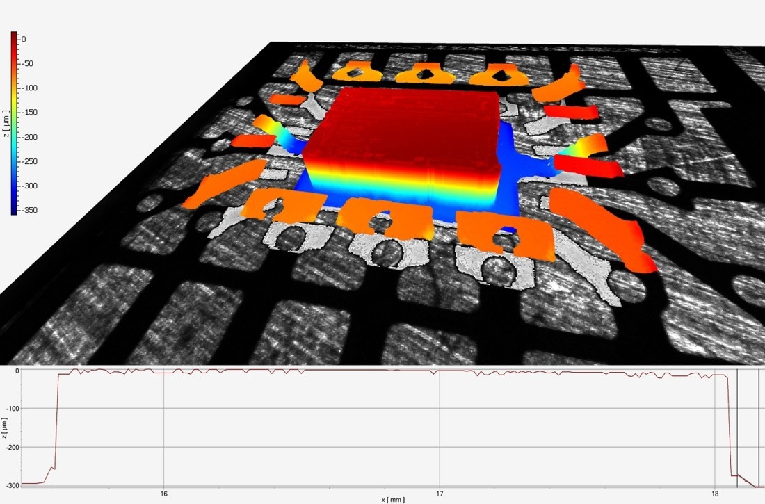
Measuring the BLT bond line thickness on an IC. Image Credit: Polytec
Epoxy die bonding chip placement positioning quality control. Image Credit: Polytec
Areal surface characterization can determine bond line thickness, slope angle for monitoring the die attach process. Image Credit: Polytec
Bond Line Thickness, Film and Layer Thickness Measurement in 3D
Layer and film thickness measurement | TopMap - optical 3D surface metrology
Video Credit: Polytec
Further Applications
Flexible Electronics
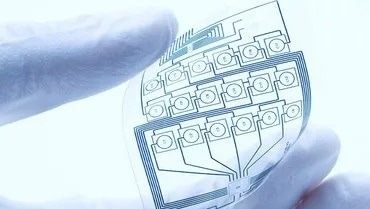
Image Credit: Polytec
Ball Grid Array (BGA)
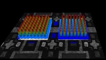
Image Credit: Polytec
High Power Laser Diodes
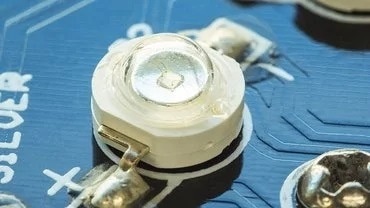
Image Credit: Polytec
Mobile Devices

Image Credit: Polytec
Pass/Fail Analysis
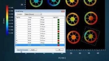
Image Credit: Polytec
Surface Roughness
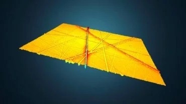
Image Credit: Polytec
Layer Thickness
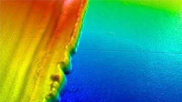
Image Credit: Polytec
Surface Parameters
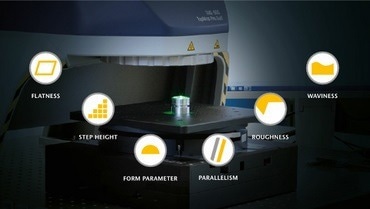
Image Credit: Polytec

This information has been sourced, reviewed and adapted from materials provided by Polytec.
For more information on this source, please visit Polytec.