Dec 4 2019
Metalenses are flat surfaces that focus light using nanostructures. Now, they are set to redefine displays, sensors, cameras, and microscopy, among other things.
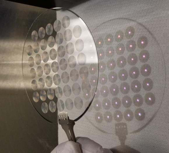
 45 1 cm metalenses on a silicon wafer focus light on a sheet of paper. Image Credit: Joon-Suh Park/Harvard SEAS.
However, to date, a majority of the lenses resemble just the size of a piece of glitter. While such small-sized lenses are suitable for certain applications, a lens of larger size is required for low-light conditions, like VR applications, where the lens has to be larger than a pupil, and an imaging system onboard orbital satellites.
At the Harvard John A. Paulson School of Engineering and Applied Sciences (SEAS), scientists have successfully created an all-glass, centimeter-scale metalens in the visible spectrum. This metalens can be produced using traditional chip fabrication techniques. The study has been published in the Nano Letters journal.
This research paves the way for so-called wafer level cameras for cell phones, where the CMOS chip and the metalenses can be directly stacked on top of each other with easy optical alignment because they are both flat. In the future, the same company can make both the chip and the lenses because both can be made using the same technology: lithography.
Federico Capasso, Robert L. Wallace Professor of Applied Physics and Vinton Hayes Senior Research Fellow, Electrical Engineering, Harvard SEAS
Capasso is the senior author of the study.
“Previously, we were not able to achieve mass-production of centimeter-scale metalenses at visible wavelengths because we were either using electron-beam lithography, which is too time consuming, or a technique called i-line stepper lithography, which does not have enough resolution to pattern the required subwavelength-sized structures,” stated Joon-Suh Park, the study’s first author and a PhD candidate at SEAS.
To manufacture a centimeter-scale metalens at the commercial level, the scientists employed a method known as deep-ultraviolet (DUV) projection lithography. This method is often utilized to pattern very fine lines as well as shapes in silicon chips in all kinds of products, ranging from mobile phones to computers.
The DUV technique can create several metalenses for each chip, where each metalens contains millions of nanoscale elements with a single shot of exposure, just like capturing a photo.
The scientists subsequently etched the nanostructure pattern directly onto the surface of the glass and thus eliminated the time-intensive deposition processes needed for the earlier types of metalenses. The new metalens is the first mass-producible, centimeter-scale, all-glass product that works in the visible spectrum.
Although this is a chromatic lens, that is, not all the different colors of light are focused at the same spot, the scientists are investigating achromatic metalenses of large diameter.
The study was co-authored by Shuyan Zhang, Alan She, Wei Ting Chen, Peng Lin, Kerolos M. A. Yousef, and Ji-Xin Cheng. It was partially supported by the Defense Advanced Research Projects Agency.
The project was partly carried out at the Center for Nanoscale Systems at Harvard University and the Cornell NanoScale Science & Technology Facility, both of which are members of the National Nanotechnology Coordinated Infrastructure (NNCI) supported by the National Science Foundation.