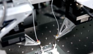
In a demonstration setup, PI (Physik Instrumente) shows how fast and precise XYZ stages are able to achieve parallel fiber alignment on the input and output side.
 Demonstration setup for component testing with two multiaxis position systems for simultaneous fiber alignment
Silicon photonics creates new challenges both for the production of components as well as testing them prior to wafer dicing. Although the test procedure is essentially the same as the familiar electrical process, it is nevertheless more sophisticated for optical components as far as precision is concerned.
The components for processing and transmitting optical signals have one or more inputs and outputs. The packaging or testing process requires an optical fiber to be adjusted with an accuracy of only a few tenths of a nanometer for each individual input and output. If the so-called alignment process is sequential, it quickly becomes uneconomical due to the time factor. As a result, a solution is required for a simultaneous alignment process on the input and output side that shortens the test duration of the components.
Compact Multiaxis Piezo Systems for Nanopositioning and Fast Fiber Alignment
In a demonstration setup, a waveguide integrated in the wafer is simulated by a single-mode fiber. Fibers with lenses are coupled at the fiber ends via precision piezo-based XYZ stages. The positioning systems have a fast scanning velocity and are able to perform alignment in several degrees of freedom – simultaneously at the input and output.
The travel ranges along the X, Y and Z axis are 25 mm for initial alignment of the fibers and 100 µm for the position-controlled scan. The modular E-712 motion controller platform with integrated alignment routines serves as controller, which was specially adapted for this task and can control six motorized and six piezo actuator axes.