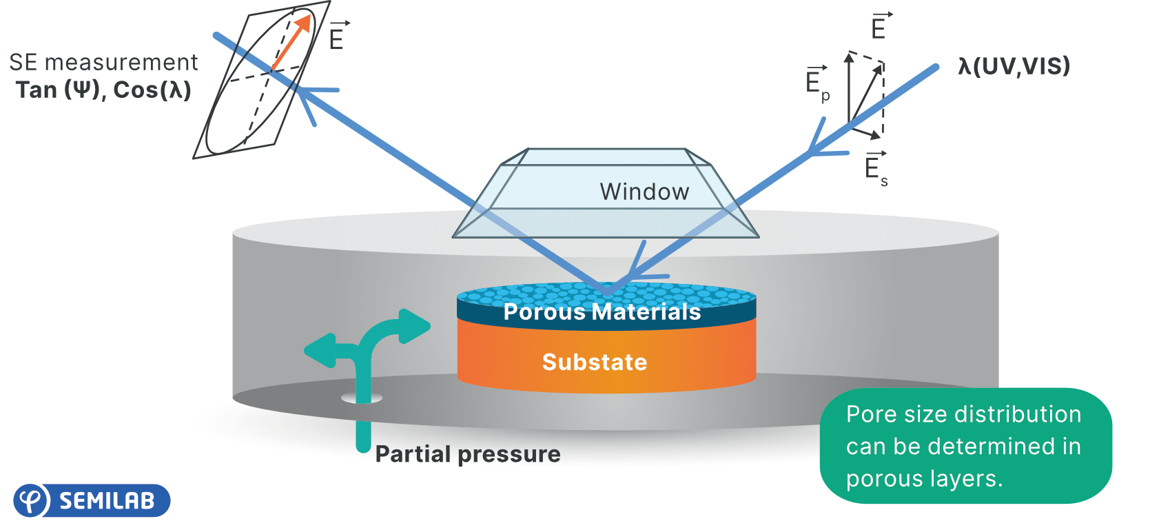
Ellipsometry Porosimetry (EP) is a technique used to measure the thickness of materials, evaluating how optical properties change throughout adsorption and desorption of a volatile species.
Depending on the application in question, this technique is performed under reduced pressure (EP) or at atmospheric pressure (EPA).
The EP technique is distinct due to its ability to measure the porosity of thin films as low as 10 nm. This technique also offers a good measurement speed and high levels of reproducibility.
Ellipsometer porosimeters are highly suited for working with extremely thin film pore size and pore size distribution measurements, particularly when compared to traditional porosimeters.
Film porosity is an essential factor in silicon-based technology that utilizes low k materials. It is also important in the organics industry, where applications are working with encapsulated OLEDs, and in the coating industry in applications utilizing SolGel techniques.
Ellipsometry Porosimetry (EP) technology was patented by IMEC and is currently licensed exclusively to Semilab.

Image Credit: Semilab Semiconductor Physics Laboratory
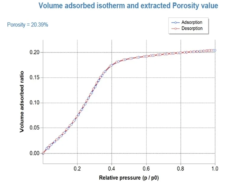
When employed during the adsorption cycle of an organic solvent, Ellipsometric Porosimetry (EP) offers the ability to measure changes in optical properties that occur as the material’s pores are filled by the adsorptive.
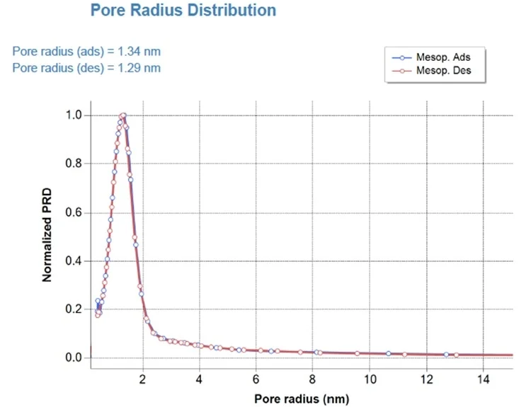
Spectroscopic ellipsometry (SE) can also be used to measure the thickness of porous thin films. A range of layer properties can be ascertained by measuring the refractive index and thickness behaviors exhibited during the adsorption cycle. These include:
- Porosity
- Hydrophobicity (water penetration)
- Young’s Modulus
- Characteristic pore size
- Pore size distribution
- Diffusion coefficient
Semilab recommends two types of adsorption cycle setup, depending on the application in question:
- At atmospheric pressure, (EPA) using water as a solvent
- Under vacuum, (EP) using a range of different organic adsorptives; for example, Methanol, Ethanol, Toluene, IPA and water
This technique is able to accommodate both meso porosity (2 > Pore diameter > 50 nm) and micro porosity (Pore diameter < 2 nm). Depending on the specific instrument configuration, it is possible to measure layers from 10 nm to several µm.
Unlike a traditional porosimeter, EP does not require sample preparation or film scratching. It is highly suited for use with very thin film pore size and pore size distribution measurements.
EP offers excellent reproducibility and measurement speed, and the technique is distinct due to its ability to measure the porosity of single and multi-layered thin film structures.

Image Credit: Semilab Semiconductor Physics Laboratory

Image Credit: Semilab Semiconductor Physics Laboratory
Applications
The EP technique offers a range of benefits to users. Thin film porosity is a key factor in silicon-based technology that employs low k materials or porous silicon films. It is also central to organic electronic applications where the permeability of the barrier layer for OPV or OLED (encapsulation) is essential.
EP is useful when working with photovoltaic technology that utilizes metal oxides (such as SiO2, TiO2 and W2O3.) for dye-sensitized solar cells. It is also highly beneficial when used in the coating industry, particularly in applications making use of the SolGel technique.
Features
The EP technique is able to provide reliable, precise measurement of a range of key parameters. These include:
- Pore size distribution and Young’s Modulus of porous thin films; for example, ultra-low K porous silicon, metal oxides, nanoparticle layers, or barrier layers
- Porosity
- Thickness
- Sealing efficiency
- Refractive index
- Diffusion coefficient

This information has been sourced, reviewed and adapted from materials provided by Semilab Semiconductor Physics Laboratory.
For more information on this source, please visit Semilab Semiconductor Physics Laboratory.